本次美国代写是集成电路的一个assignment
1. [Dynamic Behavior of Complementary CMOS] This is a follow-up problem for homework 4 problem
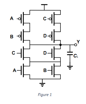
4. Using the same circuit (as shown in Figure 1) and the size of NMOS and PMOS obtained from the previous question:
(a) Suppose the equivalent resistance of single PMOS and single NMOS are 𝑅𝑅𝑃𝑃 = 2𝑅𝑅𝑁𝑁 = 𝑅𝑅 when they have size W/L = 1. Ignore the capacitance of internal nodes. Calculate the delay for the worst cases.
(b) Calculate the logic effort 𝑔𝑔 of the circuit when compared to the inverter with an NMOS
(W/L)NMOS = 1 (W/L)PMOS = 2
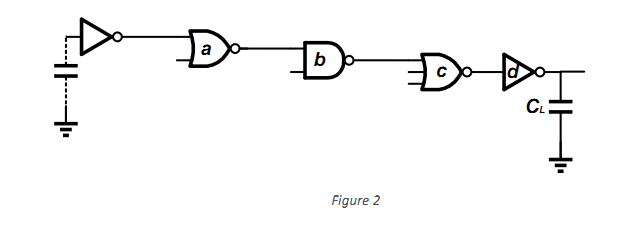
2. [Dynamic Behavior of Complementary CMOS] Consider the logic network in Figure 2, the output of the network is loaded with a capacitance 𝐶𝐶𝐿𝐿 = 5𝐶𝐶. And the input capacitance of the first gate, which is a minimum-sized inverter, is 𝐶𝐶𝑔𝑔1 = 𝐶𝐶 (𝐶𝐶𝑔𝑔1 is the capacitor on the dotted line). The effective fan-out of the path thus equals 𝑓𝑓 = 𝐶𝐶𝐿𝐿/𝐶𝐶𝑔𝑔1 = 5. Size the logic path 𝑎𝑎, 𝑏𝑏, 𝑐𝑐, 𝑑𝑑 that minimizes the path delay.